|
|
|
MY CPP PROJECT AUTOMATIC DEVICE CONTROLLER
HARDWARE IMPLEMENTATION
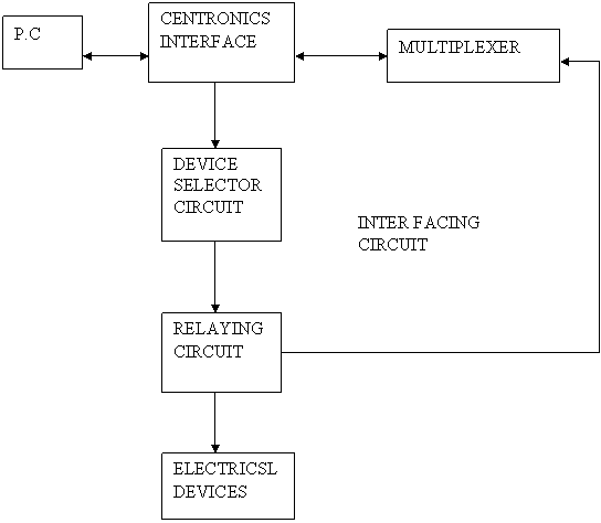
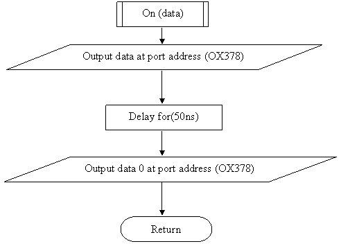
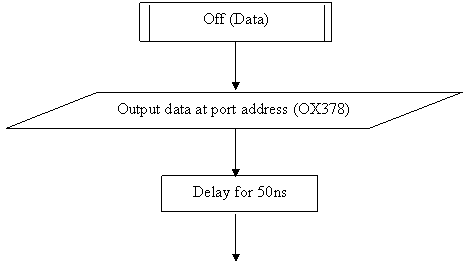
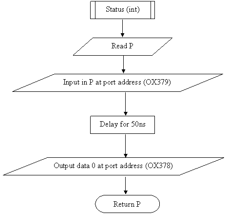
The printer port of the PC terminates to 25 pins D connector. It consists of 8 data output pin (pin no 2 to 9 for data bits Do to D7) pertaining to port with address 378hex. In case this port with base address 378h (referred to as LPT, port) is not available on the PC we can use an alternate port with base address 278h or 3BCh after checking the availability of these printer port using MSD utility program in DOS Port 379h (or in port 279h or 3bp) in case if we are using base address 378h or 3bch) is an input only one bit i.e. D7 (pin no 11 used for busy signal during printer operation) has been used for reading the status. PC inverts this bit before reading it. Further all pins of this port are logic 1 when left unused. Thus the pin 11 is made high the port will read 127 (decimal) and when pin 11 is made low, the port will read 255(decimal) pin no 18 through 25 are ground pins. This usage of various pin / data-bits of output and input port in this project is summarized below. PORT PIN No. DATA BIT USAGE 378H 2-4 D0 �D2 For outputting the address of device 378h 6 D4 For outputting the ON/OFF (I/O) state 378h 7 D5 For turning Monostable ON/OFF(I/O) 379h 11 D7 For inputting status of addressed device 18-25 Gnd To be merged with interface ground The address of the selected device output via device D0 � D2 of port 378h is decoded by 3 of 8 decoder IC (74LS138) only the output corresponding to selected device goes active low, output D0 from IC1 is not used deliberately. The address of the selected device is thus numerically equal to the weightage of the binary address bits itself. For switching ON /OFF of the address device, data bit D5 is always made logic 1. This causes mono flip flop IC3 (74LS121) to produce a pulse of approximate 5ms duration with the timing component values. The low to high going pulse from pin6 (Q0 ) of IC3 after passing through NOR buffer N5, is logically OR ed with the decoded active low outputs of decoder IC1 in seven NOR gates (NI through N4 and N6 through N8) of IC9 and IC10 (74LS02). The output of only one (out of seven) NOR gates corresponding to the address device, outputs a low to high going pulse having the same pulse width as that of the mono flip flop. This acts as a clock as a clock for corresponding D latch formed out of four 74LS74 (dual D edge triggered flip flop) IC�s(5 through 8). The D inputs of all latches that are shorted together are connected to D4 bit (representing ON/OFF state of the address selected device) .i.e. pin 6 of 25 pin �D� connector. Since the clock is available to only one (addressed / selected) flip-flop. The switch state (ON / OFF) is reflected at the output of only the concerned device flip-flop and this is used for switching ON /OFF the relay assigned to the specific device via Darlington driver forming part of IC4 (ULN2003). A logic low at the output of ULN2003 indicates that the relay pertaining to selected device is on, and vice verse. The state (on/off) of the unselected devices remains unaffected (i.e. D latched to the previous state). The outputs forms ULN2003 (IC4) are also used from the sampling the state of the device by connecting them to the seven inputs (11 through17) of 8-input multiplexer 74LS151(IC2). Input I0 is not used as done earlier in case of O0 output of 74LS138 decoder (IC1). The negative output of IC2 (at pin6) is connected to busy pin 11 (bit D7) of port 37 Ah while address of the device whose status is to be cheeked is input to IC2 in parallel with IC1. For expanding the system to switch on / off up to say 15 devices one may use additional address line (D3 ), after replacing IC1 with 74LS154 and IC2 with 74LS150 and adding additional latches and NOR Gates. The seven high current / voltage Darlington transistor arrays (ULN2003) are capable of passing up to 500mA of collectors currents. These can be driven with TTL logic inputs and the supply voltage can go up to 30V. As each output is provided with freewheeling diode internally, external diodes across relays are not required. The circuit requires 5V and 12V supplies externally for operation of the interface circuit and the relay respectively. The supply are tapped from a spare socket of the SMPS (Single mode Power supply) itself.
APPLICATIONS: 1. Can be used in Factories and Industries 2. Can be used for Domestic appliances 3. Places where No of Devices are high 4. Places where automation is required 5. STREET LIGHT CONTROLS
| |
INTRODUCTION: Consider a person who suddenly remembers that he left the washing machine at home, but decides calmly that he would switch it off once he get to his office all this thought the internet. This is exactly what I intend to do and made an attempt to this project.
DESCRIPTION
SOFTWARE DESCRIPTION
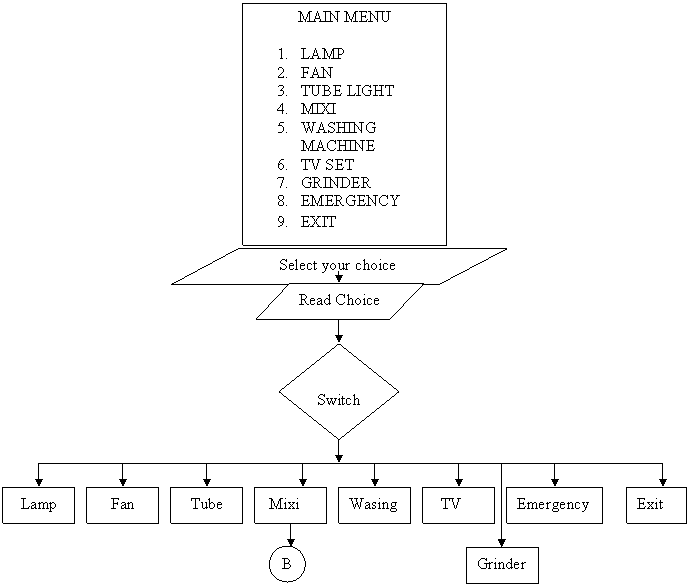
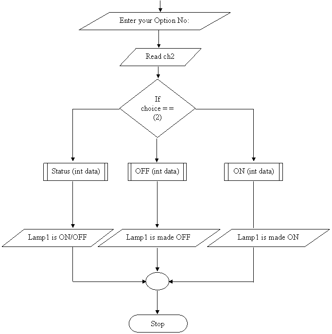
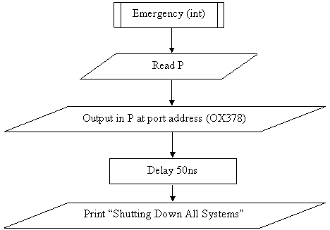
The software consists of graphics commands . Before assembling the program it has to be made sure that suitable graphic driven program, such as �EGAVGA.BGI�, is available on the PC. The main interface commands used are Outprotb (port address, data) Inportb (port address) The outportb command outputs from printer outport (hex 378 or decimal 888) the desired data. If output port is to be logic 1, the data to be output will be hex or decimal is 255. The inportb command is used to get the binary data byte from the specified input port (hex 379 or 889) since pin 11 (busy of the printers port) is used here for checking the status (while other pins of this input port are the status (while other pins of this input port are left open / unused), the value of status byte returned will be either decimal 127 (when addressed / selected device for checking the status is �ON� or 255 (when device is �OFF�) A short program is given below for independently checking and printing the data returned when pin 11 of 25 pin connector is externally made logic O (may be shorted to ground pin25) and logic 1 (may be connected to 5 V or even open as it is internally pulled high). # include <stdio.h> # include <dos.h> main( ) { int p; p=inportb(0x379); printf(�%d�,p); } The value returned with pin 11 log 1(or open) and logic 0(or ground) should be accordingly substituted in the program �P= =� in the status function for �ON� and �OFF�. Status respectively suitable comments are include in the program to make it self-explanatory. When the program is run on the PC a box containing Project member details and guide�s detail�s appears on the screen on pressing any key the following main menu appears in the screen. SELECT THE DEVICE 1. LAMP 2. FAN 3. TUBE 4. MIXI 8. Emergency shutdown 9. Quit
Please Enter the Number: Following screen will appear if selection is made 1,
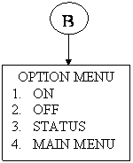
LAMP
1 ON 2 Off 3 Status 4 Main Menu
Enter the Number: Following screen will appear if selection is made 2, FAN 1 ON 2 Off 3 Status 4 Main Menu
Enter the Number: Following screen will appear if selection is made 3,
TUBE LIGHT 1 ON 2 Off 3 Status 4 Main Menu Even though when the program is terminated the status of the device remains unaltered. The status of the device change only when the power to the PC is down.
|
| DETAILS |
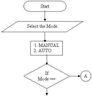
ARCHITECTURE: FLOW CHART: SCREEN 1
SCREEN 2
SCREEN 3
SCREEN 3 (OPTION 2)
SCREEN 3 (OPTION 3)
SCREEN 3 (OPTION 4)
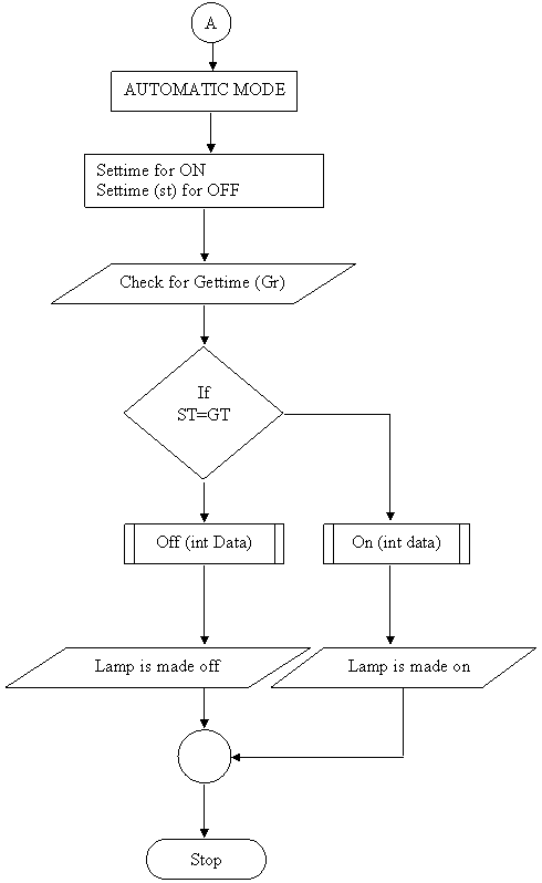
SCREEN 1 (AUTOMATIC MODE)
|
WARNING: DON'T REPUBLISH ANY CODE/PICTURE WITHOUT MY PERMISSION.
MY JAVA PROJECT
MY B.E. PROJECT
ENERGYMETER INTERFACE WITH WEBSERVER